Field Emission Auger Microprobe JAMP 9500F
(JEOL, Japan)
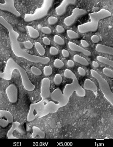
Auger Microprobe JAMP 9500F has the world’s highest spatial resolution to date. Its high performance electron optical system allows to achieve the minimum probe diameter of 3 nm in Secondary Electron Image (SEI) mode and 8 nm for Auger analysis mode. It allows surface image observation using high resolution SEI, Auger image analysis and line profile analysis. This instrument can perform depth profile analysis while employing ion etching. Moreover, a new neutralizing ion gun makes Auger analysis of insulating materials possible. Auger Microprobe JAMP 9500F is equipped with Energy Dispersive X-ray Spectrometer INCA PentaFETx3 (Oxford Instruments, UK) and Microfocus X-ray Tube with Capillary Optics µIFG iMOXS (Institute for Scientific Instruments, Germany). Its main components are shown in Fig below.
Available Techniques:
Main Auger Microprobe JAMP-9500F’s features include:
Types of researches, which we provide:
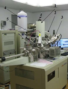
Field Emission Auger Microprobe JAMP-9500F (JEOL, Japan): High Resolution Scanning Electron Microscope with Field Emission Electron Gun (1); Auger Electron Spectrometer (2); Ar-Ion Gun (3); Energy Dispersive X-ray Spectrometer INCA PentaFETx3 (Oxford Instruments, UK) (4); Microfocus X-ray Tube with Capillary Optics µIFG iMOXS (Institute for Scientific Instruments, Germany) (5).
